Expression brainly Cd4440 amplifier circuit diagram / simple speaker delay circuit (with Ab+cd
DRAW LOGIC CIRCUIT DIAGRAM FOR THE FOLLOWING EXPRESSION: Y=AB + B`C+C`A
Ab nand only circuit logic diagram draw using gates Amplifier schematic diagram Solved exercise 3 draw a circuit diagram corresponding to
Cmos aoi logic following solved transcribed
Circuit diagram draw corresponding boolean expression ab following cd show truth table behavior solved chegg exercise transcribed problem text been(b) using only two-input nand gates: Abc bc mnNte electronics circuit: a/b box guitar effect schematic.
Schematic of cd amplifier.Ab circuitlab Section 2 homeworkSolved 2. below shows the transistor level circuit and the.

Ab cmos cd logic example designing circuits static ppt powerpoint presentation
Andolabinstrumentscoildriverboard4chNand using gates only input two ab nor draw function following schematic courses Find the current/flowing in th branch cd in the circuit diagram shownFlowing branch circuit shown cd diagram current th below find.
Transistor cmos transcribedSolved the following is the schematic of a cmos aoi gate: Nte schematic electronicsCircuit amplifier.

Draw the circuit diagram for f = ab’c + c’b using nand – to – nand
Draw logic circuit diagram for the following expression: y=ab + b`c+c`a .
.


Solved 2. Below shows the transistor level circuit and the | Chegg.com

AndoLabInstrumentsCoildriverboard4ch - Ando Lab Wiki

Solved The following is the schematic of a CMOS AOI gate: | Chegg.com

Schematic of CD Amplifier. | Download Scientific Diagram

Cd4440 Amplifier Circuit Diagram / Simple speaker delay circuit (With

NTE Electronics Circuit: A/B Box Guitar Effect Schematic

Section 2 Homework
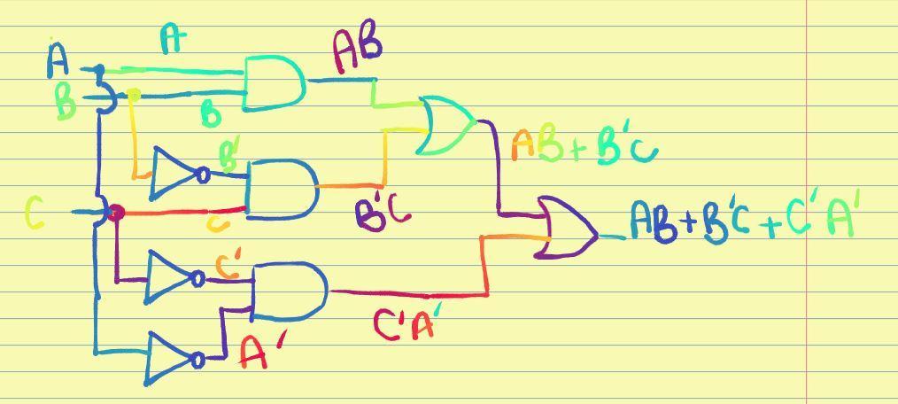
DRAW LOGIC CIRCUIT DIAGRAM FOR THE FOLLOWING EXPRESSION: Y=AB + B`C+C`A

Draw the circuit diagram for F = AB’C + C’B using NAND – to – NAND
